


一、What is PCB packaging?
PCB Encapsulation defines the physical interface between electronic components and the PCB, providing the necessary information for PCB assembly and maintenance, such as the shape and symbol of the component, the number and location of pads, reference pins, polarity, and so on.
Each component placed on the side of the PCB must have its own package, including the copper area on the PCB where the component will be soldered, e.g. a 16-pin SSOP package containing 2 rows of 8 rectangular pads each.
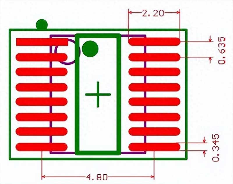
The figure below shows the footprint of a general purpose electronic component in a 16-pin SSOP package, the red part corresponds to the copper area on the layer, while the other colours represent the mechanical type layer.
二、What are the types and sizes of PCB packages?
There are several types of PCB packages, the most common being:
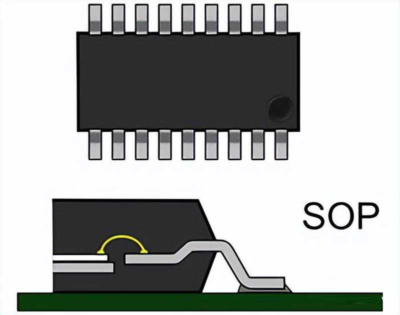
1、 SOP (Small Outline Package)
The smallest footprint used for integrated circuits (ICs), usually about 0.4″ x 0.4″.
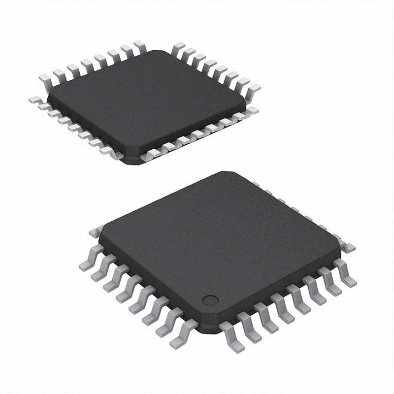
2、QFP (quad flat package)
Larger PCB footprint for ICs and integrated circuits, usually about 0.8″ x 0.8″, but can be as large as 1″ x 1″.
3、BGA (Ball Grid Array)
This is a larger PCB package for ICs and ICs with many connections. They are usually rectangular in shape with pins on all sides, allowing them to be placed in any orientation. Size varies greatly depending on the number of connections per IC; sizes range from 0.5″ x 0.5″ to over 2″ x 2″.

三、PCB Package Contains What Information?
1、Pads / Holes
Used to indicate the assembly of SMD components pads or holes used to fix the location of through-hole components, which is critical to the soldering, must be precisely defined.
2、Outline of the component
Can be defined as the protected area of the PCB package in which other components can be placed placed, the boundary defines the entire body of the component and is responsible for defining the main layers of the component shape.
3、Reference Indicator
That is, a letter, number code, used to uniquely identify the schematic and PCB layout components, the following figure shows some reference indicators, for example, R3 resistors and C5 capacitors.
4、Pin 1 Indicator
When placing components with a large number of pins (such as integrated circuits), it is important to indicate the location of pin 1 on the package to avoid possible misunderstandings at the assembly stage. This is the case, for example, for components with QFP or DIP packages. This can be a white circle, a triangle, or a square, as shown below.

5、Mechanical Information
Some components may have some mechanical parts, or protrusions that may extend over other components, creating possible collisions or overlaps between components. For example, a heat sink.
6、3D Models and Symbols
Each PCB package has an associated symbol in the schematic and, in most cases, an associated 3D model. This allows designers to create a 3D model of the entire board, verifying proper positioning and distances between components.

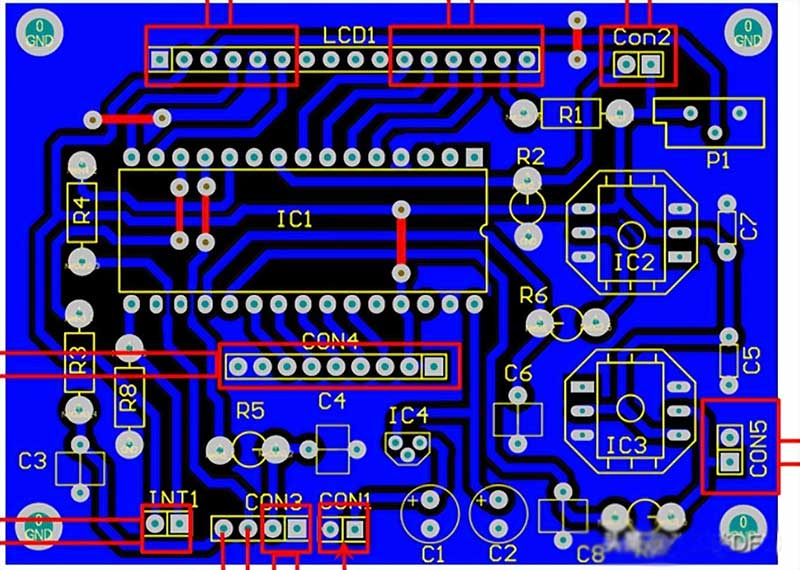
The figure below, shows the complete PCB, associated with the open source project containing highly integrated SMD components (FPGAs). Looking at the packages of all these components, in addition to the arrangement and relative spacing of the pads, a dot (or a circle) is included to identify pin 1. We can also note that in the case of the X1 oscillator, the component symbol is displayed.

四、PCB Encapsulation Standards
For PCB packaging, there are specific internationally applicable standards for defining packages, schematic symbols and 3D models.
1、IPC 7351 (PCB package)
The IPC 7351 standard (specifically, IPC-SM-7351-B) defines a set of equations that control the size of the pads around a component. Components complying with IPC 7351 will be designed in accordance with these standards.
2、ANSI Y32.2-1975 (schematic symbols)
This standard defines a list of graphical symbols used in electrical and electronic drawings and a series of category name letters. Some CAD tools engineers can set up themselves, but most CAD tools are default.
3、ISO 10303-21 (3D Models)
The ISO 10303-21 standard defines the file format used for STEP models that can be imported into 3D CAD software. The standard is more of a file format specification than a requirement for drawing component packages.

五、Design PCB package to follow the rules
1、Pad Size
Pad size must be suitable for component leads or pins, and must allow safe soldering and electrical connections. PCB pad size is usually specified in the component data sheet, or you can use the IPC-7351B and other PCB design standards to determine.
2、Pad Spacing
The spacing between pads must be suitable for component leads or pins, and must allow proper soldering and electrical connections. Pad spacing is also specified in the component data sheet or determined using PCB design standards.
3、Pad Shape
The shape of the pads must match the shape of the component leads or pins, and must allow safe soldering and electrical connections. The shape of the pad is specified in the component data sheet or determined using PCB design standards.
4、Through-Hole Placement
For through-hole components, the placement of the through-hole must be accurate to ensure that the components are properly aligned and securely connected. The location of the through-hole is usually specified in the component data sheet or determined using PCB design standards.
5、Reference Marks
Reference markers must be placed correctly to ensure clear and accurate component identification. The placement of reference indicators is usually specified in the component data sheet or determined using PCB design standards.
6、Clearance and Creepage Distance
Clearances and creepage distances between components and the rest of the PCB must be sufficient to prevent electrical shorts and ensure safe operation. The minimum required clearance and creepage distance is usually specified in industry standards such as IPC-7351B or IPC-SM-782.
7、Alignment Width
The alignment width must be appropriate for the current flowing through the alignment to ensure a stable and reliable electrical connection. The width of an alignment is typically determined using design rules that take into account voltage and current levels as well as the length and temperature of the alignment.
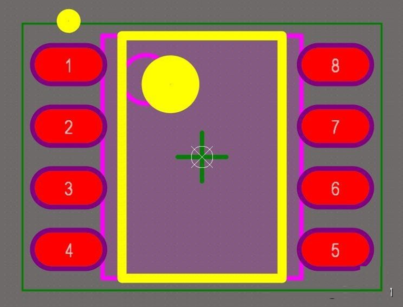
An example of the correct PCB package is shown.
- The yellow layer of l contains the silkscreen and Pin 1 reference;
- l The red layer contains pad definitions;
- l The purple layer contains the definition of the mechanical dimensions;
- l And the green layer contains the definition of the outline.
The above is about PCB packaging.