


As NPI engineers, DFM manufacturability analysis involves a very wide range, today is mainly to solve the problem: how many layers of PCB board is better? How to determine the number of PCB layers?
一、What is the meaning of PCB layers?
PCB layer is the copper layer, PCB is made of copper + substrate compression and become, in addition to a single panel is a layer of copper, double-sided boards are more than double layer. Components are soldered on the outermost layer, the other layers play a role in connecting wires, but now there are some high-end PCB will be buried in the PCB components inside the inner layer.
PCBs are used to manufacture a wide range of electronic devices and machinery in different industries such as consumer, automotive, telecoms, aerospace, military and medical. The number of layers and size of a particular board determines the power and capacity of the PCB. As the number of layers increases, so does the functionality.

二、How to determine the number of PCB layers?
When you consider how to choose the number of PCB layers, you need to think, what are the benefits of multilayer over single/double layer? On the contrary, you also need to think about the benefits of single layer compared to double / multilayer where? Specifically, you can consider the following 5 aspects:
1、PCB used for where?
When considering the needs of PCB boards, you need to consider the machines and equipment that the PCB will be used in, but also to determine the requirements of these machines/equipment on the circuit board circuit. Is it used for high-tech, complex electronic products or simple products with fewer functions?

2、PCB need what operating frequency?
Here you need to consider the issue of operating frequency. Because the parameters of the operating frequency determines the function and capacity of the PCB. For higher speed and operating capacity, multi-layer PCB is essential.
3、What is the project budget?
Other factors to consider are the manufacturing costs of single and double layer PCBs versus multi-layer PCBs. If you want PCBs with the highest possible capacity, then the cost to be paid will definitely be relatively high.
Some people ask: the relationship between the number of PCB layers and the price, usually the higher the number of layers, the higher the price will be. Because the design and manufacture of multi-layer PCBs will be longer, the cost will be higher. The average cost of multi-layer PCBs from 3 manufacturers is listed below:
The cost criteria for the charts are as follows:
- PCB Order Quantity: 100;
- PCB size: 400 mm x 200 mm;
- Number of layers: 2, 4, 6, 8, 10.
The chart below shows the average price of PCBs from 3 manufacturers, excluding shipping costs. Here you can use a PCB quoting website, which can help to evaluate the cost of the PCB and also to select different parameters. For example, conductor type, size, quantity, number of layers, and so on.
The graph shows the average price of PCBs from three different companies, but it should not be taken as an absolute value, but rather to understand how the price increases according to the number of levels. Obviously, shipping costs are not included in the calculation. Effective calculators are available online, produced by the manufacturers themselves, which help customers to evaluate the cost of their printed circuits, choosing different parameters such as type of conductor, size, quantity, number of layers, insulation, thickness, etc.

Average cost chart of PCB with different number of layers
4、How long is the delivery time required for PCB?
Delivery time, is the time required to manufacture single/double/multi-layer PCB boards, when you need to manufacture PCB boards in large quantities, you need to consider the delivery time. The delivery time for single/double/multi-layer PCB boards is not the same, it also depends on the size of the PCB board area. Of course, if you are willing to spend more money, then the delivery time may also be shortened.
5、PCB need what density and signal layer?
The number of PCB layers also depends on the pin density and signal layers, for example: 1.0 pin density requires 2 signal layers, and as the pin density decreases, the number of layers required will increase. If the pin density is 0.2 or less, a minimum of 10 PCB layers is required.

三、The number of PCB layers – single / double / multi-layer advantages
1、Single-layer PCB
Single-layer PCB construction is very simple, single-layer PCB consists of a layer of laminated and soldered dielectric conductive material layers. It is first covered with a copper laminate and then with a soldermask. Illustrations of single-layer PCBs usually show three colour bars indicating the layer and its two overlays – grey for the dielectric layer itself, brown for the copper laminate and green for the soldermask.

Advantages
- Low manufacturing costs. Especially cost-effective for the production of consumer devices.
- Components are easier to drill, solder and mount and are less likely to cause production problems.
- Affordable and easy to mass produce quantities.
- Ideal for low density designs.
Applications:
- Calculators, the most basic calculators use a single layer PCB.
- Radios, such as low cost radio alarm clocks from general supply shops, typically use a single layer PCB.
- Coffee makers, coffee makers typically use a single layer PCB.
- Household appliances, some household appliances, on the use of single-layer PCB.
2、Double-layer PCB
2-layer PCBs are copper-plated on both sides with an insulating layer in the middle, and there are components on both sides of the board, which is why it is also known as a double-sided PCB.They are manufactured by joining two layers of copper together, with dielectric material in the middle, and each side of the copper can carry different electrical signals for applications that require high speeds and compact packages.
Electrical signals are routed between the two layers of copper, and the dielectric material between them helps prevent these signals from getting in the way of each other. 2-layer PCBs are the most common, and the most economical boards to manufacture.

A two-layer PCB is much like a one-layer PCB, but with an inverted, mirrored bottom half. With a two-layer PCB, the dielectric layer is thicker than a single layer. In addition, the dielectric is laminated with copper on both the top and bottom surfaces. In addition, the top and bottom of the laminate are covered with soldermask.
Illustrations of two-layer PCBs usually look like a three-layer sandwich with a thick grey layer in the middle representing the dielectric, brown bars at the top and bottom representing the copper, and thin green bars at the top and bottom representing the soldermask.
Pros:
- The flexibility of thedesign makes it suitable for a wide range of devices.
- The low cost construction of makes it convenient for high volume production.
- Simple design of.
- Small size makes it suitable for a variety of devices.

Dual-layer (aka double-sided) PCBs at the design stage. traces are routed on top (red) and bottom (blue)
Applications:
Two-layer PCBs are suitable for a variety of simple and more complex electronic devices. Examples of mass manufacturing equipment that incorporate two-layer PCBs include:
- HVAC units, various brands of residential heating and cooling systems contain two-layer printed circuit boards.
- Amplifiers, two-layer PCBs equipped with amplifier units used by numerous musicians.
- Printers, a variety of computer peripherals rely on two-layer PCBs.
4、Four-layer PCBs
A 4-layer PCB is a printed circuit board with four conductive layers: a top layer, two inner layers and a bottom layer. The two inner layers are the core and are typically used as power or ground planes, while the top and bottom outer layers are used to house components and route signals.
The outer layer is usually covered with a soldermask with exposed pads to provide placement points to connect surface mount devices and through-hole components. Through-holes are typically used to provide connections between the four layers, forming a board when they are laminated together.
The following is a breakdown of these layers:
Layer 1: The bottom layer, usually made of copper. It serves as the foundation for the entire board and provides support for the other layers.
Layer 2: The power supply layer. It is so named because it provides a clean and stable power source for all the components on the board.
Layer 3: The ground plane layer, which acts as a ground source for all components on the board.
Layer 4: The top layer is used to route signals and provide connection points for components.
This is the standard 4-layer PCB stack arrangement, but can be switched depending on the design specification and the layer with the most signals.
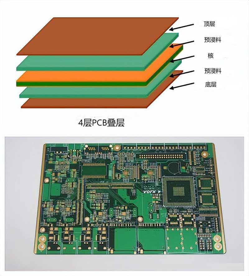
In a 4-layer PCB design, 4 copper strips are separated internally by 3 layers of internal dielectrics and sealed at the top and bottom by a soldermask. Typically, the 4-layer PCB design rule is illustrated with 9 strips and 3 colours – brown for copper, grey for core and prepreg and green for soldermask.
Pros:
- Durability – Four layer PCBs are more robust than one and two layer boards.
- Compact Size – The small design of the four-layer PCB can fit a variety of devices.
- Flexibility- Four-layer PCBs can work in many types of electronic devices, both simple and complex.
- Safety – Four-layer PCBs are shielded from electromagnetic interference by properly aligning the power and ground layers.
- Lightweight-Devices equipped with a four-layer PCB require less internal wiring and are therefore typically lighter in weight.
Applications:
- Satellite Systems – Multi-level PCBs have been equipped for satellites in orbit.
- Handheld Devices – Mobile phones and tablets are typically equipped with a four-layer PCB.
- Space Exploration Equipment- Multi-layer PCBs power space exploration equipment.
5、Six-Layer PCBs
A 6-layer PCB is essentially a 4-layer board with 2 additional signal layers added between the planes. 6-layer PCBs have a standard stack consisting of 4 wiring layers (2 outer and 2 inner) and 2 inner planes (one for ground and one for power).
Providing 2 internal layers for high-speed signals and 2 external layers for low-speed signals significantly amplifies EMI (Electromagnetic Interference), which is the energy that destroys signals in electronic devices by radiation or induction.

6-Layer PCB
6-layer PCB stacks can be arranged in a variety of ways, but the number of power, signal and ground layers used depends on the application requirements.
A standard 6-layer PCB stack consists of top layer – prepreg – internal ground layer – core – internal wiring layer – prepreg – internal wiring layer – core – internal power layer – prepreg – bottom layer.
Whilst standard, this arrangement is not suitable for all PCB designs and it may be necessary to reposition layers or have more specific layers. However, placement must take into account wiring efficiency and crosstalk minimisation.

Pros:
- Strength – Six-layer PCBs are thicker than their thinner-layer predecessors and are therefore stronger.
- Compactness – Boards of this thickness with six layers have greater technical capacity and therefore can consume less width.
- High capacity- PCBs with six or more layers provide optimum power for electronic devices and greatly reduce the potential for crosstalk and EMI.
Applications:
- Computers – Six-layer PCBs have helped drive the rapid development of personal computers, which have become more compact, lighter and faster.
- Data Storage – The high capacity of 6-layer PCBs has enabled data storage devices to become increasingly abundant over the past decade.
- Fire Alarm Systems – Using six or more layers of circuit boards, alarm systems have become more accurate the moment a real danger is detected.
6、Complex Multilayer PCBs
As the number of layers in a multilayer printed circuit board increases beyond the fourth and sixth layers, more layers of conductive copper and dielectric material are added to the stack.
For example, an eight-layer PCB contains four planar and four signal copper layers – eight in total – connected together by seven rows of dielectric material. The eight-layer stack is sealed at the top and bottom with a dielectric soldermask. Basically, an eight-layer PCB stack is much like a six-layer stack, but with the addition of a pair of copper and prepreg columns.
The trend continues with the 10-layer PCB, which adds two layers of copper for a total of six signal layers and four planar copper layers – 10 in all. Bonding the copper in the 10-layer PCB stack are nine columns of dielectric material – five columns of prepreg and four cores. The 10-layer PCB stack is sealed with dielectric resistive solder layers at the top and bottom like all other stacks.
When it comes to the 12-layer PCB stack, the board has four planar and eight signal conductive layers bonded by six signal and five dielectric core columns. 12-layer PCB stacks are sealed with dielectric resist layers. In general, the multilayer PCB illustration depicts the layers and bonding materials in the following colours – brown for signal/planar copper, grey for prepreg/core dielectric material and green for top/bottom soldermask.