一、Defects caused by PCB manufacturing and storage process
Similar to other electronics, PCB is sensitive to different environmental factors such as temperature, humidity, pollution, etc. In the manufacturing and storage process, PCB will appear various defects.
1、Temperature
In the storage process and the component installation process, PCB will be affected by temperature, in extreme conditions, the temperature will be many fluctuations, which may lead to the potential for component or connector failure.
In the PCB design stage must consider the maximum and minimum operating temperature of the PCB, due to temperature fluctuations caused by the PCB expansion and contraction can lead to premature failure of the PCB.
2、Moisture
PCB manufacturing and storage process, exposure to moisture may lead to short circuits, and may lead to defects in various components of the circuit. The presence of moisture in the air can damage the solder, which in turn leads to corrosion.
3、Contaminants
Contaminants can create defects in the manufacturing process and where the PCB is stored after the manufacturing process, when the PCB is exposed to dust, insects, pollution and other factors, it will weaken the PCB performance.
4、Influence
The impact on the PCB can be catastrophic during the manufacturing, storage and transport of the PCB. PCBs that are dropped violently or not manufactured in the normal way can cause excessive vibration, and as a result, the PCB loses its flexibility, which in turn damages the PCB’s alignment.
二、PCB soldering process defects
During the PCB soldering process, a variety of soldering defects may occur. The following are some common welding defects:
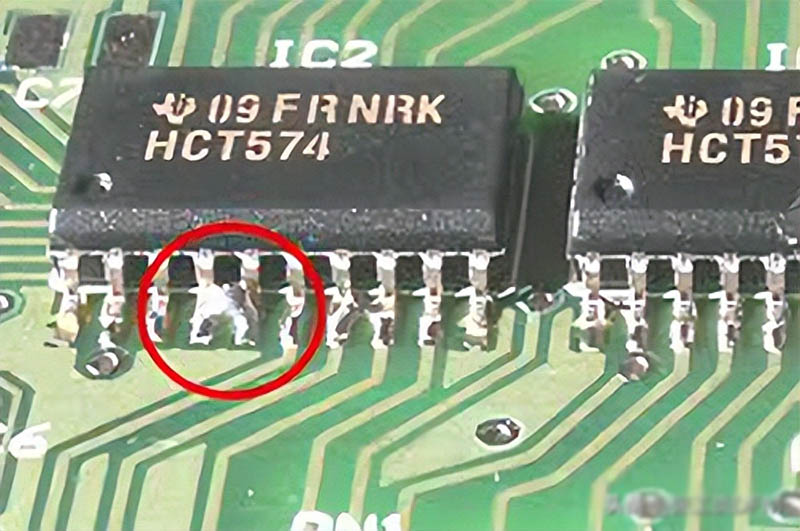
1、Open-circuit solder joints
When there is no point of contact between the solder and the PCB pad, it will result in an open-circuit solder joint. This can be caused by incorrect soldering temperature, physical movement or vibration of the PCB during transport.
2、Excessive Soldering
During the soldering process, if the soldering iron is left in contact for too long, this can lead to excessive solder build-up, increasing the risk of solder bridges and potentially causing serious damage to circuit connections.
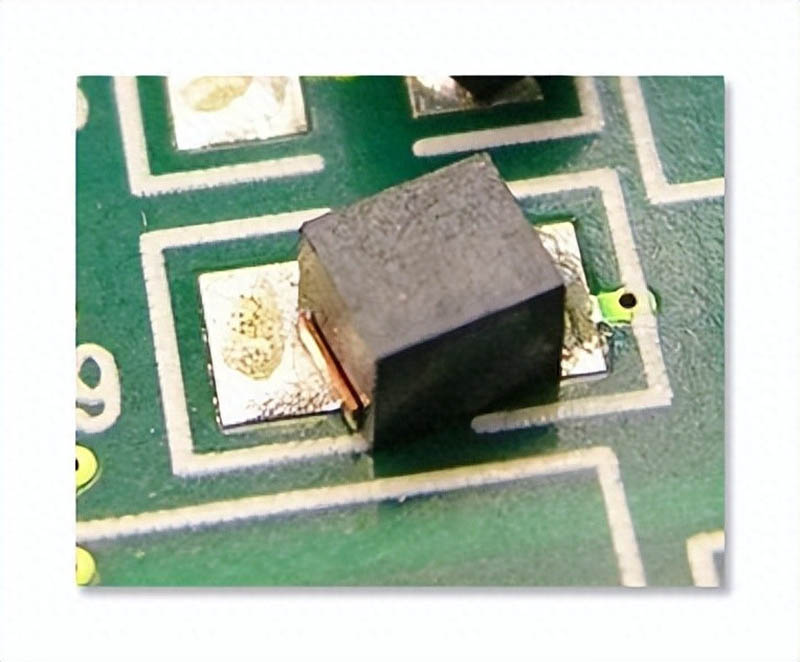
3、Component displacement
Component displacement can occur when components placed on the PCB are not properly aligned during the soldering process. This can lead to open connectors and crossed signal lines, which can cause problems in electronic circuits.
4 、Webbing and Splattering
Webbing and splattering may occur when atmospheric contaminants affect the soldering of PCBs. These defects can create a short circuit hazard and also affect the appearance of the PCB.
5、Pad Warping
When the pads are disconnected from the surface of the PCB or when the force is dispersed, it is called pad warpage. This can lead to irregular circuit connections, which in turn can lead to PCB failure.

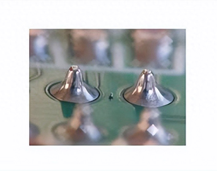
6、Solder Ball
Solder balls are caused by harsh conditions such as gases in the flux or excessive turbulence during solder reflow. A large number of solder balls may form false bridges between neighbouring alignments, leading to circuit failure.
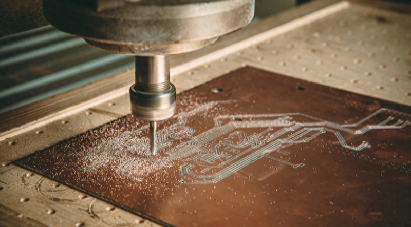
7、Mechanical defects
CNC milling machines are used to route, cut and outline PCBs during the manufacturing process. If the mechanical equipment operates at too high a temperature, it may lead to problems such as degradation of board quality, misalignment and edge collapse.
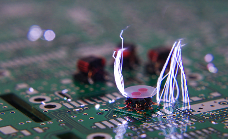
8、Defects Caused by Electrostatic Discharge
Electrostatic discharges may cause short circuits on the PCB, soften the solder and cause damage to the resistance of the components. Electrostatic discharge may be caused by man or machine, should be carefully tested in the manufacturing and assembly process.
三、 How to Find PCB Defects
In the PCB manufacturing process, each stage of the inspection is very important to help identify and correct defects in the PCB. Here are some common inspection methods:
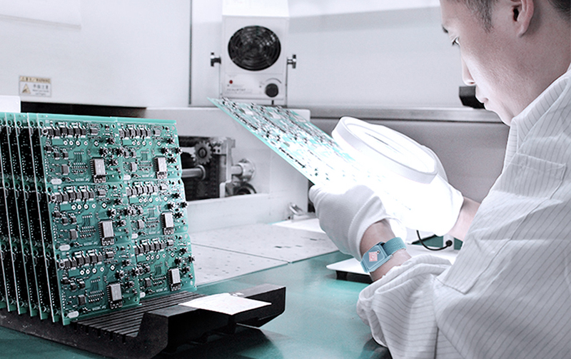
1、Visual Inspection
Visual inspection is the most common type of inspection. Visual inspection can be equipped with special equipment according to the inspection target. For example, reflow soldering points on the PCB are usually inspected with a prism, which helps to identify a variety of manufacturing defects, such as poor solder joints, uneven soldering, short circuits, open circuits and so on.
X-RAY inspection is a very useful inspection method for components, soldering, component misalignment and so on. Through X-RAY inspection, the internal structure and connection of PCB can be checked without destroying the PCB, which helps to identify the invisible defects in PCB.
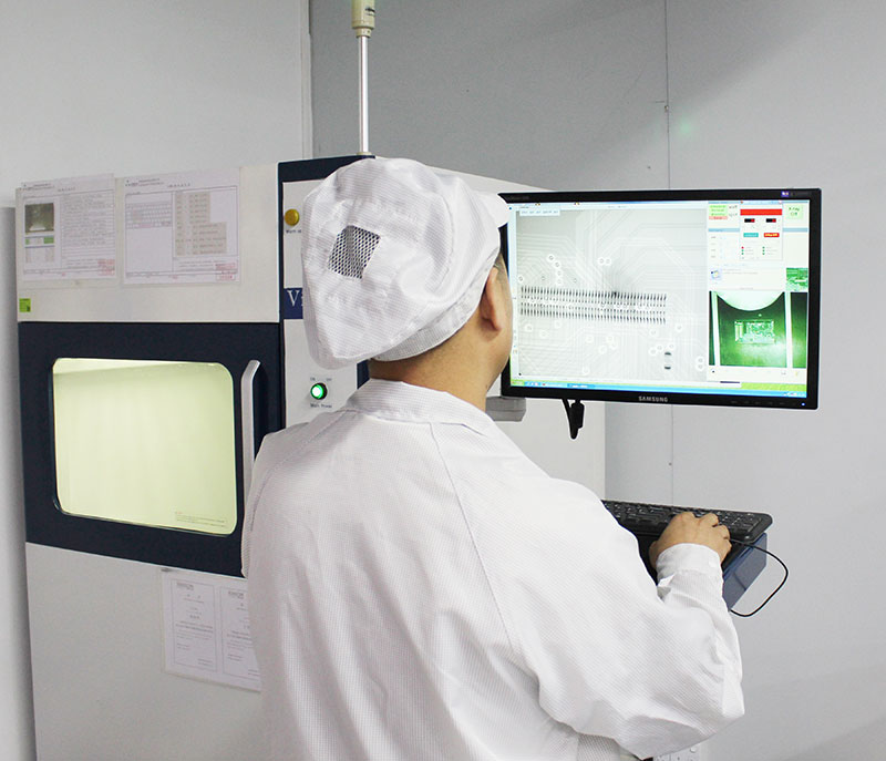
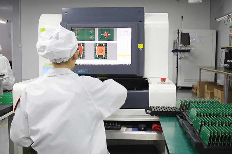
3、AOI Inspection
AOI inspection is an automatic optical inspection method that helps to detect defects such as scratches, stains, marks and other dimensional defects. Through this method, we can also identify tilted or incorrect components, which helps to improve inspection efficiency and accuracy.
4、FCT Inspection
FCT inspection, also known as functional testing, directly checks the functionality of PCBs under real environmental conditions. Through FCT inspection, the working status and performance of PCB can be checked, such as input and output, signal transmission, voltage and current. This method can ensure the reliability and stability of PCB in real applications.
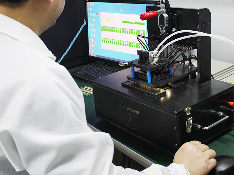
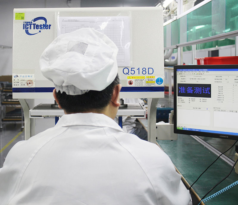
5、ICT Inspection
ICT inspection is an inspection method based on electrical testing, which can check for defects such as short or open circuits, soldermask defects, misplaced or missing components, and so on. Through ICT inspection, the electrical performance and connection of PCB can be quickly detected, which helps to improve the manufacturing efficiency and quality of PCB.